Researchers Demonstrate a Practical Path Toward Stacked Silicon Logic Chips
The semiconductor industry has spent years discussing the promise of monolithic 3D integrated circuitsA semiconductor technology that stacks multiple layers of silicon transistors vertically within a single chip to increase density and performance.. The concept is straightforward: instead of arranging transistors side-by-side across a flat silicon surface, stack multiple layers of transistors vertically. The result could be dramatically higher transistor density, shorter signal paths, reduced power consumption, and significantly more computing capability within the same chip footprint.
The challenge has never been the idea itself. The challenge has been manufacturing.
Researchers at the University of Illinois Urbana-Champaign recently reported a breakthrough that may help overcome one of the biggest barriers to practical 3D silicon chips. Their work, published in Nature, demonstrates a method for stacking multiple layers of silicon transistors while avoiding the high-temperature processing that traditionally damages circuitry already fabricated on lower layers.
Why Technology is Chasing 3D Chips
For decades, the semiconductor industry has relied on shrinking transistor dimensions to improve performance and efficiency. However, as process technologies approach physical limits, continued scaling becomes increasingly expensive and difficult.
Three-dimensional integration offers an alternative path forward.
Instead of making transistors smaller, engineers can build upward. Similar to constructing a skyscraper rather than expanding horizontally, multiple layers of circuitry can occupy the same footprint while providing substantially more computing resources.
The approach has attracted interest for applications ranging from AI accelerators and advanced processors to next-generation memory technologies. Readers familiar with 3D NAND flash memory will recognize a similar concept of building upward rather than outward, although the new research focuses on stacking logic transistors rather than memory cells.
The Problem They Are Trying To Solve
Traditional silicon transistor fabrication requires process steps that involve temperatures exceeding several hundred degrees Celsius.
When building a second or third transistor layer above an existing circuit, these temperatures can damage the completed structures underneath.
Previous research attempted to address this issue by replacing silicon with alternative semiconductor materials that can be processed at lower temperatures. While these approaches reduced thermal stress, they often sacrificed performance, limiting their commercial appeal.
The Illinois team chose a different strategy.
Instead of abandoning silicon, they found a way to continue using it.
Thin-Silicon Might Become The Solution
The researchers developed ultra-thin silicon sheets approximately 10 nanometers thick.
To appreciate how thin this is, a human hair is typically around 80,000 to 100,000 nanometers wide.
These silicon filmsUltra-thin layers of silicon used in advanced semiconductor manufacturing for stacking transistors vertically. are peeled from a specially prepared substrate and transferred onto an existing chip structure using a rolling transfer process. The entire operation occurs at temperatures below 200°C, well within the safe thermal limits of previously fabricated circuitry.
Once transferred, the team creates transistor structures using a design that avoids the high-temperature processing normally associated with conventional silicon devices.
The result is a multi-layer silicon architecture that preserves the performance advantages of traditional silicon technology while meeting the temperature requirements of monolithic 3D integration.
Is the Tape the Breakthrough?
One aspect of the research that attracted attention was the mention of adhesive tape being used to separate the ultra-thin silicon sheets from their source substrate.
At first glance, this may sound like the central innovation. It is not.
The tape functions primarily as a transfer mechanism. Similar transfer techniques have been used in various advanced materials applications for years.
The true breakthrough lies elsewhere:
- Producing silicon layers thin enough to be transferred without damage
- Maintaining high-performance silicon characteristics
- Performing the transfer at temperatures compatible with existing circuitry
- Achieving the precision required for multi-layer chip fabrication
The adhesive simply helps move the silicon from one location to another.
In commercial production, the transfer mechanism could eventually evolve into a different process entirely while preserving the core technology.
Alignment Is Everything For 3D Chips
Perhaps even more impressive than the transfer process is the reported alignment accuracy.
According to the researchers, successive silicon layers can be aligned within less than 10 nanometers.
This detail may prove more significant than the transfer method itself.
Modern integrated circuits rely on billions of precisely positioned features. When multiple transistor layers are stacked, electrical connections must line up with extraordinary accuracy. Even slight misalignment can prevent circuits from functioning correctly.
Achieving sub-10-nanometer alignment suggests the process may be capable of supporting the dense vertical interconnections required by future commercial devices.
While the research paper does not fully detail every alignment technique used, semiconductor manufacturing typically employs alignment marks, high-resolution optical systems, nanometer-scaleRefers to dimensions or structures measured in nanometers, typically on the order of billionths of a meter. positioning stages, and advanced lithography methods to achieve this level of precision.
The flexibility of the ultra-thin silicon sheets may also contribute by allowing them to conform closely to the underlying surface, reducing mechanical imperfections during placement.
Prelim Results
To validate the concept, the team fabricated working three-layer memory structures.
According to the researchers, the stacked design reduced circuit area by as much as three times compared with an equivalent planar implementation.
The fabricated devices also demonstrated electrical characteristics comparable to conventional silicon transistors, suggesting that performance need not be sacrificed to achieve three-dimensional integration.
So What Is Next?
Although the results are promising, significant challenges remain before the technology reaches commercial production.
Laboratory demonstrations are typically performed on relatively small samples under carefully controlled conditions. Semiconductor manufacturers must eventually scale the process to large production wafers while maintaining yield, reliability, throughput, and cost targets.
Nevertheless, the research represents an important milestone.
The semiconductor industry already possesses decades of expertise, manufacturing infrastructure, and supply chains built around silicon.
The industry’s experience scaling vertically stacked memory devices provides some confidence that complex three-dimensional manufacturing can eventually reach production. Recent examples include Micron’s 232-layer 3D NAND technology, which demonstrated how aggressively modern semiconductor manufacturers can scale vertical structures.
A successful path toward monolithic 3D circuits that preserves silicon compatibility could be considerably more attractive than transitioning to entirely new materials.
For now, the work serves as an encouraging indication that the future of chip scaling may not depend solely on making transistors smaller. Instead, the next major leap in computing performance could come from stacking silicon circuits vertically and transforming today’s flat chips into true three-dimensional systems.
As AI workloads, high-performance computing, and data center demand continue to grow, advances such as these may ultimately determine how much additional performance the semiconductor industry can deliver in the decade ahead.
3D Chip Overview – Image
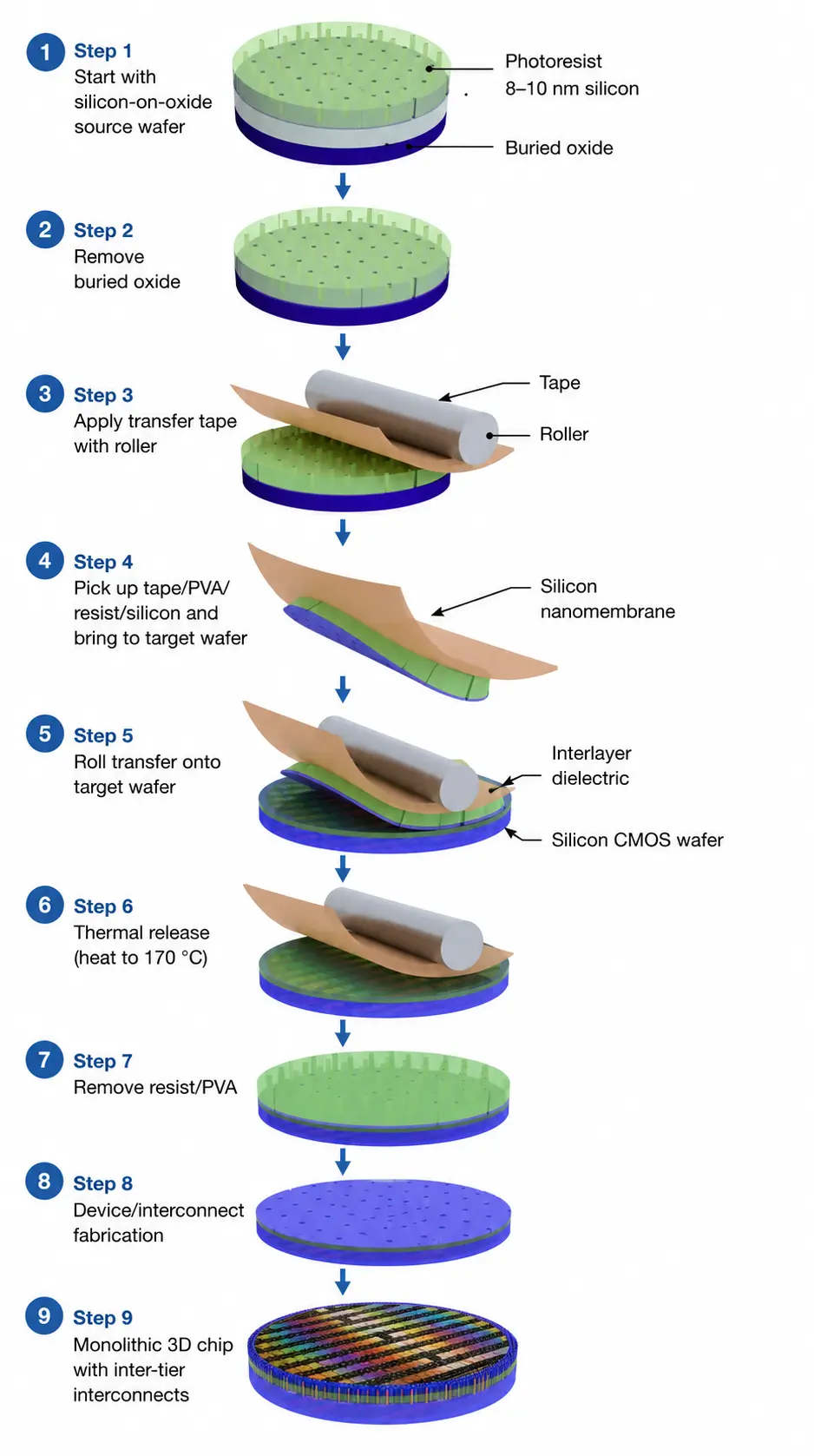
Monolithic 3D Silicon Chip Fabrication Process
View Detailed Process Table
| Step | Process | Purpose |
|---|---|---|
| 1 | Prepare silicon-on-oxide source wafer | Create an ultra-thin silicon layer on a donor substrate. |
| 2 | Remove buried oxide layer | Release the silicon nanomembrane from the source wafer. |
| 3 | Apply transfer tape with roller | Attach the ultra-thin silicon layer to a temporary carrier. |
| 4 | Lift and transport silicon nanomembrane | Move the silicon layer to the destination wafer. |
| 5 | Roll-transfer onto target wafer | Position the silicon nanomembrane onto the CMOS wafer and dielectric layer. |
| 6 | Thermal release at 170°C | Separate the transfer tape without damaging underlying circuitry. |
| 7 | Remove resist and PVA layers | Expose the transferred silicon layer for device fabrication. |
| 8 | Fabricate devices and interconnects | Build transistors and vertical connections between layers. |
| 9 | Complete monolithic 3D chip | Produce a stacked silicon integrated circuit with inter-tier interconnects. |
Editorial Note: This article was prepared as a technology news update based on recently published semiconductor research and related reporting. The explanation was written for a technical audience and reviewed for clarity around monolithic 3D integration, silicon transistor stacking, low-temperature transfer methods, and alignment challenges.