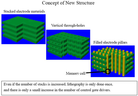
Toshiba might be on to something with their development of a new three dimensional memory cell array structure that enhances cell density and data capacity without relying on advances in process technology. All this with minimal increase in chip size.

The new structure design reflects pillars of stacked memory elements passing vertically through multi-stacked layers of electrode material and utilize shared peripheral circuits. The design is a potential candidate technology for meeting future demand for higher density NAND flash memory.
Typically, advances in memory density reflect advances in process technology, but Toshiba’s approach isn’t necessarily the case.
Toshiba’s new approach is based on innovations in the stacking process, not manufacturing process. Existing memory stacking technologies simply stack two-dimensional memory array on top of another, repeating the same set of processes.

While this achieves increased memory cell density, it makes the manufacturing process longer and more complex. The new array design from Toshiba does increase memory cell density, is easier to fabricate, and does not require increase in chip area, as peripheral circuits are shared by several silicon pillars.
Toshiba said that it will further develop this elemental technology to the level where it matches current structures in terms of security and reliability. So nothing concrete yet, but well on the way with Toshiba’s announcement and commitment to fine-tuning this approach. With computer hard drives starting to go NAND based, there is a lot at stake.
Source: Aving USA News

